What is latch?

SR Latch | NOR and NAND SR Latch
Ⅰ.What is latch?
A latch is a type of pulse-sensitive memory cell circuit. They have the ability to change state in response to a certain input pulse level. Latching is the process of momentarily storing a signal in order to maintain a specific level state. The latch's primary job is to cache data, followed by solving the asynchronous problem of the high-speed controller and slow peripherals, the driving problem, and ultimately the problem of an I/O port that can both output and input. Level control data input is used in latches, which include latches without enabling control and latches with enabling control.
Ⅱ.What’s the function of the latch?
Latch is a type of pulse-sensitive memory cell circuit. They have the ability to change state in response to a certain input pulse level. Latching is the process of momentarily storing a signal in order to maintain a specific level state. The latch's primary job is to cache data, followed by completing high-speed management of the asynchronous problem with sluggish peripherals, solving the driving problem, and finally solving the problem of an I/O port that can both output and input data.
Ⅲ.What’s the working principle of the latch?

Working Principle of latch
Components:
D Flip-Flop: Core storage element.
AND, OR, NOT gates: Logic operations.
Clock (C): Synchronization signal.
Inputs: D (Data), C (Clock), C̅ (Inverted Clock).
Outputs: Q (Stored data), Q̅ (Inverted Output).
Connections:
The D input is connected to the AND gate and other logic components.
The Clock signal (C) is used to trigger state changes.
The output Q represents the stored data and is connected to various components.
The Q̅ (inverted Q) output provides complementary output.
Latches operate on level-triggered principles:
Data Capture: Input state is stored when the enable signal is active
Data Retention: Output maintains its state until new data is latched
State Maintenance: Stored value remains stable independent of input changes
(Pedroni, 2020)
In the case of LED and digital tube displays, it is frequently necessary to refresh continually and quickly in order to maintain a data display. Particularly on strobed display systems, such as four-segment eight-digit digital tubes. It will be refreshed every 30 milliseconds, which is within the human-acceptable refresh frequency. This takes up a lot of the processor's processing time, uses a lot of the processor's processing power, and wastes a lot of the processor's power.
In this case, latches can significantly reduce the processor's workload. When the CPU transfers data to the latch and latches it, the latch's output pin remains in the data state until new data is latched. In this method, the processor's processing time and the IO pin can be released while the digital tube's display information remains unchanged. The processor's processing time is clearly confined to when the display content changes, which is only a small portion of the total display duration. After processing, the processor will have more time to do other things. The latch serves this purpose in LED and digital tube displays: it saves important MCU time.
Ⅳ.Where can latch be used?
The term "latch" refers to the fact that the state of the output terminal does not change with the state of the input terminal, and that the input state is only saved to the output when a latch signal is present, and that it is not changed until the next latch signal arrives.
Integrated circuits make the most use of latches. In digital circuits, they are utilized as store elements in sequential circuits. Latches are sometimes utilized as data registers in arithmetic circuits.
It can be utilized independently after being packed as a standalone product, and the data is effectively delayed while the clock signal is valid. This means that the clock signal is sent first, followed by the data signal.
In some applications, an external latch on the microcontroller's I/O port is necessary. To achieve address multiplexing, for example, when a single-chip microcomputer is coupled to off-chip memory, a latch must be connected. Assuming that the MCU port's 8 I/O pins are used for both address and data signals, the address can be latched using a latch. (Specific operation: send the address information first, which will be locked at the address end of the peripheral by the ALE enable latch, then send the data information and read and write enable signals, and read and write at the given address)
If the single-chip microcomputer's bus interface is only used for one purpose, no latch is required; if the single-chip microcomputer's bus interface is utilized for two purposes, a latch is required. For example, two LEDs must be controlled by an I/O port. When transmitting data to the first LED, "open" the first latch and "lock" the second latch to save the data. When transmitting data to the second LED, "open" the second latch while "locking" the first latch to preserve the data on the first LED. Three latches can be employed if one port of a single-chip microcomputer is to be used for three functions, and the operation method is comparable. The latch can be thought of as an expander of the microcontroller's I/O port in this case.
Real-World Uses
1 Display systems include LED screens.
• Seven-segment, multi-digit displays
• Management of refresh rate (usually 30 ms cycles)
• Reduction of processor workload
2 Digital systems include state machines, data registers, memory buffers, and sequential circuit elements (Tocci et al., 2019).
Ⅴ.The role and difference between latches and buffers
The latch's purpose is to keep the current state locked so that the data sent by the CPU stays at the interface circuit's output for a period of time and the state does not change until the lock is released. Latches are found on several chips. The 74LS244 chip, for example, has a latching capability. The output will remain in its current state when a pin is set high, and it will not change until the pin is cleared.
Buffer registers are also known as buffers, and they are divided into input and output buffers. The former's job is to temporarily store data sent by the peripheral so that the processor may retrieve it; the latter's job is to temporarily store data sent by the processor to the peripheral. The numerical control buffer allows the high-speed operating CPU to coordinate and buffer the slow-functioning peripherals in order to achieve data transmission synchronization. The buffer must have a three-state output function because it is connected to the data bus.
Ⅵ.Commonly used 74 series latch chip introduction
1. 74-series
This is an older product that is still in use but is being phased out gradually.
2. 74H-series
This is a more advanced version of the 74-series, a high-speed TTL product. The NAND gate's average transmission time is roughly 10ns, yet the circuit's static power consumption is quite high. This series of items is currently utilized less and less and is being phased out.
3. 74S-series
This is TTL's Schottky high-speed series. Anti-saturation Schottky diodes are utilized in this series, which have a faster speed but fewer variations.
4. 74LS-series
In the current TTL type, this is the major product line. There are numerous manufacturers and varieties to choose from. Because of its great performance-to-price ratio, it is currently commonly employed in tiny and medium-sized circuits.
5. 74ALS-series
The "advanced low-power Schottky" series is what it's called. It is a successor product to the 74LS-series, with substantially enhanced speed (average value of 4ns), power consumption (typical value of 1mW), and other features, but at a rather high price.
6. 74AS-series
This is the successor of the 74S-series, with major improvements in speed (average value of 1.5ns), and is also known as the "advanced ultra-high-speed Schottky" series.
7. 74HC-series
Like 74HC259, the 54/74HC family of high-speed CMOS standard logic circuits feature the same workability as the 74LS series, as well as the CMOS integrated circuit's inherent low power consumption and wide power supply voltage range. With the identical serial number, 74HCxxx is a duplicate of 74LSxxx. The last few numbers of the model are identical, suggesting that the logic function and pin configuration of the circuit are totally equivalent, making the 74LS and 74HC interchangeable.
References
Floyd, T. L. (2021). Digital fundamentals (12th ed.). Pearson.
Mano, M. M., & Ciletti, M. D. (2022). Digital design: With an introduction to the Verilog HDL (6th ed.). Pearson.
Morris, J. M., & Ciletti, M. D. (2021). Digital design and computer architecture (3rd ed.). Morgan Kaufmann.
Pedroni, V. A. (2020). Circuit design with VHDL (3rd ed.). MIT Press.
Tocci, R. J., Widmer, N. S., & Moss, G. L. (2019). Digital systems: Principles and applications (12th ed.). Pearson.
Wakerly, J. F. (2017). Digital design: Principles and practices (5th ed.). Pearson.
1.What is the difference between a latch and a flip-flop?
The latch is related to all its input signals. When the input signal changes, the latch changes and has no clock terminal; the flip-flop is controlled by the clock, and only when the clock is triggered, the current input is sampled and the output is generated.

The latch is triggered by level and controlled asynchronously. The latch is equivalent to the path when the enable signal is valid, and the latch maintains the output state when the enable signal is invalid. The flip-flop is triggered by a clock edge and is controlled synchronously.

The latch is sensitive to the input level and is greatly affected by the wiring delay. It is difficult to ensure that the output is free of glitches; the flip-flop is not easy to produce glitches.
2.What is the "second state" in the latch?
Q refers to Qn (original state), and Q* refers to Qn+1 (secondary state), which means that Qn+1 is the state of Qn at the next moment.
Simply put, the "second state" refers to: the next state.
3. What are the functions of the LE and OE of the latch?
Latch Enable: Latch enable, when it is invalid, the output will not change and maintain the original value.
Output Enable: The output is enabled. When it is invalid, the output is in a high-impedance state.
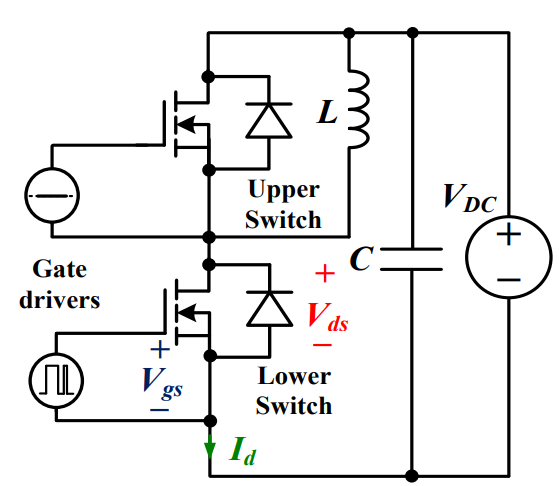
 Discovering New and Advanced Methodology for Determining the Dynamic Characterization of Wide Bandgap DevicesSaumitra Jagdale15 March 20242470
For a long era, silicon has stood out as the primary material for fabricating electronic devices due to its affordability, moderate efficiency, and performance capabilities. Despite its widespread use, silicon faces several limitations that render it unsuitable for applications involving high power and elevated temperatures. As technological advancements continue and the industry demands enhanced efficiency from devices, these limitations become increasingly vivid. In the quest for electronic devices that are more potent, efficient, and compact, wide bandgap materials are emerging as a dominant player. Their superiority over silicon in crucial aspects such as efficiency, higher junction temperatures, power density, thinner drift regions, and faster switching speeds positions them as the preferred materials for the future of power electronics.
Read More A Comprehensive Guide to FPGA Development BoardsUTMEL11 September 202514676
This comprehensive guide will take you on a journey through the fascinating world of FPGA development boards. We’ll explore what they are, how they differ from microcontrollers, and most importantly, how to choose the perfect board for your needs. Whether you’re a seasoned engineer or a curious hobbyist, prepare to unlock new possibilities in hardware design and accelerate your projects. We’ll cover everything from budget-friendly options to specialized boards for image processing, delve into popular learning paths, and even provide insights into essential software like Vivado. By the end of this article, you’ll have a clear roadmap to navigate the FPGA landscape and make informed decisions for your next groundbreaking endeavor.
Read More Applications of FPGAs in Artificial Intelligence: A Comprehensive GuideUTMEL29 August 20253606
This comprehensive guide explores FPGAs as powerful AI accelerators that offer distinct advantages over traditional GPUs and CPUs. FPGAs provide reconfigurable hardware that can be customized for specific AI workloads, delivering superior energy efficiency, ultra-low latency, and deterministic performance—particularly valuable for edge AI applications. While GPUs excel at parallel processing for training, FPGAs shine in inference tasks through their adaptability and power optimization. The document covers practical implementation challenges, including development complexity and resource constraints, while highlighting solutions like High-Level Synthesis tools and vendor-specific AI development suites from Intel and AMD/Xilinx. Real-world applications span telecommunications, healthcare, autonomous vehicles, and financial services, demonstrating FPGAs' versatility in mission-critical systems requiring real-time processing and minimal power consumption.
Read More 800G Optical Transceivers: The Guide for AI Data CentersUTMEL24 December 20253830
The complete guide to 800G Optical Transceiver standards (QSFP-DD vs. OSFP). Overcome supply shortages and scale your AI data center with Utmel Electronic.
Read More Xilinx FPGAs: From Getting Started to Advanced Application DevelopmentUTMEL09 September 20254299
This guide is your comprehensive roadmap to understanding and mastering the world of Xilinx FPGA technology. From selecting your first board to deploying advanced AI applications, we'll cover everything you need to know to unlock the potential of these remarkable devices. The global FPGA market is on a significant growth trajectory, expected to expand from USD 8.37 billion in 2025 to USD 17.53 billion by 2035. This surge is fueled by the relentless demand for high-performance, adaptable computing in everything from 5G networks and data centers to autonomous vehicles and the Internet of Things (IoT). This guide will walk you through the key concepts, tools, and products in the Xilinx ecosystem, ensuring you're well-equipped to be a part of this technological revolution.
Read More
Subscribe to Utmel !
![UCC5310MCDR]() UCC5310MCDR
UCC5310MCDRTexas Instruments
![1EDI20H12AHXUMA1]() 1EDI20H12AHXUMA1
1EDI20H12AHXUMA1Infineon Technologies
![1EDI60H12AHXUMA1]() 1EDI60H12AHXUMA1
1EDI60H12AHXUMA1Infineon Technologies
![1EDI30I12MFXUMA1]() 1EDI30I12MFXUMA1
1EDI30I12MFXUMA1Infineon Technologies
![UCC21220DR]() UCC21220DR
UCC21220DRTexas Instruments
![HCS201T-I/SN]() HCS201T-I/SN
HCS201T-I/SNMicrochip Technology
![ADATE305BSVZ]() ADATE305BSVZ
ADATE305BSVZAnalog Devices Inc.
![AD9172BBPZ]() AD9172BBPZ
AD9172BBPZAnalog Devices Inc.
![ADUM4223CRWZ]() ADUM4223CRWZ
ADUM4223CRWZAnalog Devices Inc.
![FM33256B-G]() FM33256B-G
FM33256B-GCypress Semiconductor Corp


 Product
 Brand
Brand Articles
 Tools
Tools


